
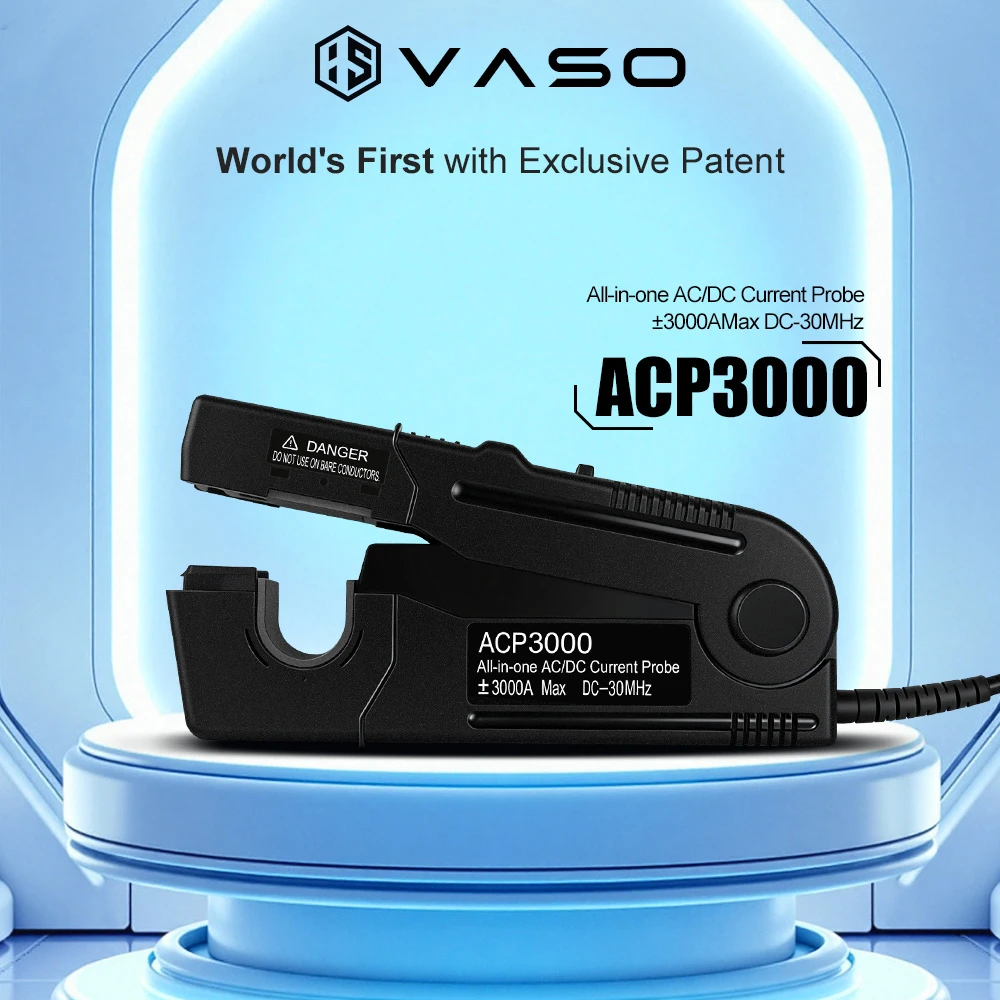
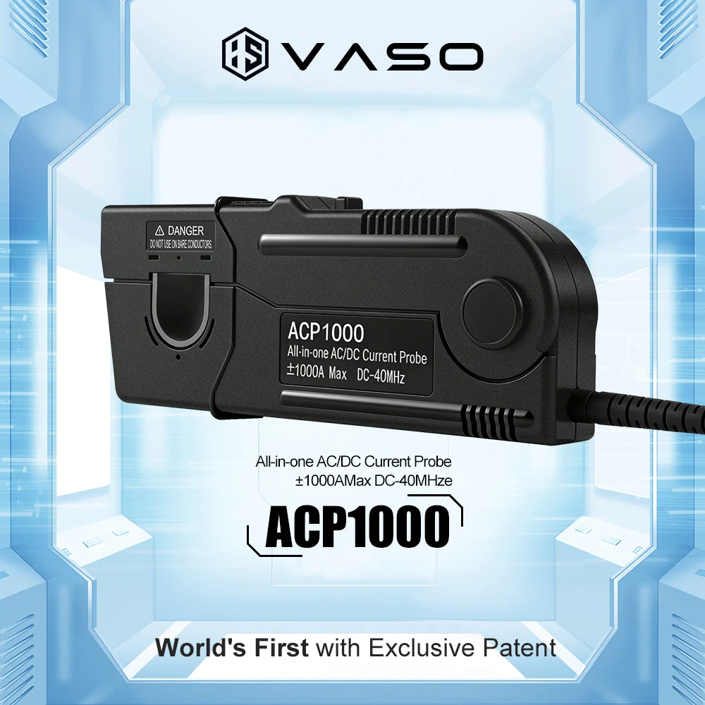
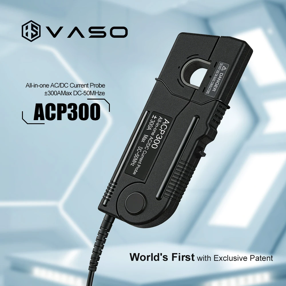
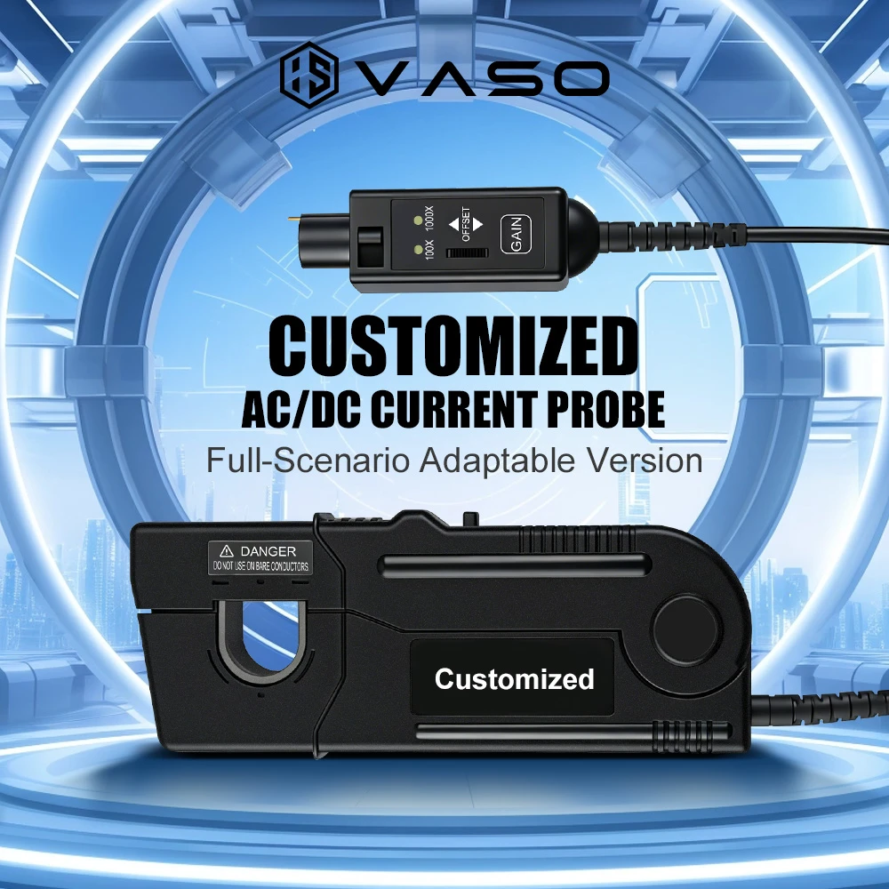
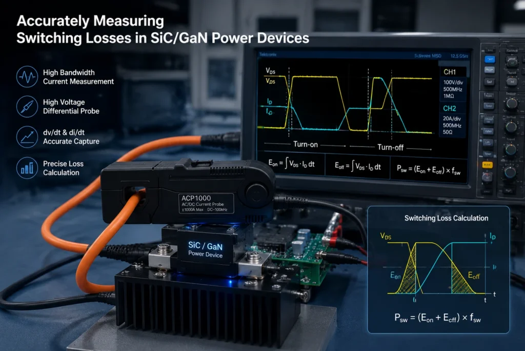
Wide-bandgap semiconductors have reset the performance envelope for power conversion. Silicon carbide (SiC) MOSFETs and gallium nitride (GaN) HEMTs switch in tens of nanoseconds rather than the hundreds of nanoseconds typical of silicon IGBTs, and they do so at higher voltages and junction temperatures. That speed is precisely what makes them attractive for EV traction inverters, onboard chargers, server power supplies, and solar string inverters — smaller magnetics, higher efficiency, higher power density. It is also what makes their switching losses genuinely difficult to measure with any confidence.
Power engineers who have tried to characterize a SiC half-bridge on a bench quickly discover that the same measurement techniques that worked fine for a 600V silicon IGBT start producing numbers that don’t add up once edge rates climb past 50 V/ns and current slew rates exceed 1-2 A/ns. The instrumentation, not just the device under test, becomes the limiting factor — and of the two channels feeding the loss calculation, current is where that limitation shows up first. A wideband AC/DC current probe, capable of resolving a fast nanosecond-scale edge without losing the underlying DC bias current it rides on, is what keeps the rest of the measurement chain honest.
Why switching loss measurement gets harder with WBG devices
Switching loss is calculated by integrating the instantaneous power — the product of drain-source (or collector-emitter) voltage and drain (or collector) current — over the turn-on and turn-off transition intervals. On paper this is straightforward. In practice, the accuracy of that integral depends entirely on how faithfully the voltage and current waveforms are captured, and three problems compound with WBG devices in particular.
Bandwidth and rise time. A SiC MOSFET turning on in 15-20 ns has spectral content well into the hundreds of megahertz. A current probe with a bandwidth of 50 MHz or 100 MHz — perfectly adequate for a silicon IGBT switching in 200-300 ns — will round off the leading edge of the transition, understate the peak current, and shift the apparent timing of the switching event relative to the voltage waveform. Any of these errors directly distorts the energy integral.
Phase and timing alignment. Because the switching interval is so short, even a few nanoseconds of skew between the voltage and current channels produces a disproportionate error in calculated Eon and Eoff. A 5 ns timing mismatch that would be a rounding error on a 300 ns silicon transition can shift a 15 ns SiC transition’s calculated loss by 20% or more. Probe-to-probe propagation delay differences, which are often ignored in silicon-era test setups, cannot be ignored here.
Insertion impedance and loop parasitics. Any current probe adds some series impedance and loop inductance to the measurement path. At the di/dt levels WBG devices produce, even a few nanohenries of added inductance generates measurable ringing and voltage overshoot that wasn’t part of the device’s native switching behavior. The probe becomes part of the circuit under test rather than a passive observer of it — which is exactly why the physical construction of the current probe, not just its bandwidth spec, has to be evaluated for WBG work.
Why the AC/DC current probe is the deciding factor
Of the two waveforms needed for a switching-loss calculation, current is by far the harder one to capture cleanly, and the choice of current probe is usually what separates a trustworthy Eon/Eoff figure from a plausible-looking but wrong one. Voltage can be measured with a well-compensated high-voltage differential probe placed close to the device terminals with minimal loop area — a comparatively mature and forgiving measurement. Current measurement has to simultaneously solve for probe bandwidth, insertion impedance, core saturation behavior, and, for devices that carry substantial DC bias current superimposed on the switching transient, the ability to resolve a fast AC edge riding on top of a large DC offset without distorting either.
This last requirement is where a purpose-built AC/DC current probe earns its place on the bench, and where a probe designed for one regime or the other falls short. A double-pulse test on a SiC or GaN device commonly involves inductor currents in the tens of amps, with the switching transition itself occurring in single-digit nanoseconds. An AC-only current transformer probe cannot report the steady-state DC component at all, since a CT has no response at zero frequency — it will show the edge but lose the baseline it’s switching from. A DC-only Hall-effect probe, on the other hand, typically lacks the bandwidth to track a 15-20 ns edge without rounding it off. Neither, used alone, produces a waveform that represents what the device actually did.
An AC/DC current probe solves this by combining both sensing elements in a single measurement path — a Hall-effect sensor providing accurate response from DC up through the low-frequency range, and a current-transformer or shunt-based path handling the fast, high-frequency content of the switching edge — with the two signals recombined internally into a single, continuous output. Done well, this produces a waveform that is flat across the entire frequency range relevant to a WBG switching event: accurate at the DC bias level the inductor is sitting at, and accurate through the nanosecond-scale transient superimposed on top of it. That combined response is what makes the resulting v(t)×i(t) power integral — and therefore the Eon/Eoff numbers derived from it — meaningful rather than an artifact of which half of the waveform the probe happened to capture well.
Because this dual-sensing architecture is doing double duty, not every AC/DC current probe on the market is equally suited to WBG work. A few specifications matter more than the headline bandwidth number on a datasheet:
- Rise time relative to the device under test. As a rule of thumb, probe rise time should be at least three to five times faster than the fastest edge being measured, so the probe’s own response doesn’t dominate the recorded transition.
- Propagation delay and delay matching. Manufacturers typically publish a fixed propagation delay figure; this needs to be known and compensated for, not assumed to be negligible.
- Low insertion impedance. Split-core clamp probes with small aperture size and short current path length minimize the added loop inductance in the switching commutation loop.
- DC offset current handling. The probe needs adequate dynamic range to capture the full DC bias current without saturating the core during the peak of the switching transient, where current can spike well above steady-state levels.
- A clean crossover between the DC/low-frequency path and the AC path. This is the specification unique to AC/DC current probes and the one most often overlooked. If the handoff between the Hall-effect and current-transformer stages isn’t well matched in gain and phase, the recombined waveform shows a bump, dip, or timing glitch right around the crossover frequency — often landing in the exact frequency range where the switching edge’s energy is concentrated.
A practical measurement workflow
Most switching loss characterization for SiC and GaN devices is done using the double-pulse test (DPT), which isolates a single turn-on and turn-off event under controlled current and voltage conditions without the thermal buildup of continuous switching. Getting trustworthy Eon/Eoff numbers out of a DPT setup generally follows a consistent sequence:
1. Deskew the voltage and current channels before taking any data. This is done by driving a known signal — often a fast edge from a pulse generator — through both the current probe and the voltage probe simultaneously using a deskew fixture, then applying a timing offset in the oscilloscope until the two edges align. Skipping this step is the single most common source of erroneous switching-loss numbers in WBG testing.
2. Position the current probe in the commutation loop with minimal added loop area. The probe should sit as close as practically possible to the device under test, ideally in the source or drain lead rather than further out in the PCB layout, to avoid capturing stray inductive ringing that isn’t representative of the device’s intrinsic switching behavior.
3. Verify probe bandwidth against actual observed edge rates, not assumed ones. It’s worth capturing a turn-on transition and checking the measured dV/dt and dI/dt against the probe’s specified bandwidth before trusting the resulting energy figures — device-to-device and gate-driver-to-gate-driver variation can push edge rates higher than expected.
4. Integrate power over a consistently defined window. Eon and Eoff are typically defined as the integral of v(t)×i(t) from the point voltage or current first departs from its steady-state value to the point both have settled to within a defined percentage of final value. Using a consistent, documented window matters when comparing loss figures across different devices, gate resistances, or temperatures.
5. Repeat across the operating envelope. Because switching loss in WBG devices is a strong function of current, bus voltage, gate resistance, and junction temperature, a single data point at one operating condition says very little about how a device will behave across the full range an application requires. Loss curves as a function of current and voltage, taken at multiple temperatures, are what feed into a realistic efficiency model.
Instrumentation choices carry through to the design
Switching loss data from bench characterization ultimately informs thermal design, heatsink sizing, and efficiency targets for the end system. An underreported Eoff figure from an under-bandwidth current probe can lead to an undersized heatsink and a thermal margin problem that doesn’t surface until the product is in the field. Conversely, measurement artifacts from excessive probe insertion inductance can make a device look worse than it actually performs, leading to overly conservative — and more expensive — thermal and derating decisions.
Given how directly these numbers feed downstream design decisions, the current probe used for switching loss characterization deserves at least as much scrutiny as the power devices themselves — and for WBG work specifically, that means an AC/DC current probe rather than an AC-only or DC-only alternative. It’s the one piece of test equipment sitting directly in the commutation path, responsible for reporting both the steady-state current the device is switching from and the nanosecond-scale transient it’s switching through, without adding its own distortion to either. Bandwidth, propagation delay, insertion impedance, DC dynamic range, and crossover quality aren’t secondary specifications for this application — collectively, they determine whether the resulting Eon/Eoff figures reflect the device under test or the limitations of the probe measuring it. Getting that one instrument right is, in a very concrete sense, what makes every downstream efficiency and thermal calculation trustworthy.